RFX8051B

CMOS 5GHz WLAN 802.11ac RFeIC WITH PA, LNA AND SPDT


Please note: RFX8051B is being discontinued and is not recommended for new designs. The suggested replacement is SKY85712-11


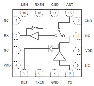
RFX8051B is a highly integrated, single-chip, single-die RFeIC (RF Front-end Integrated Circuit) which incorporates key RF functionality needed for IEEE 802.11a/n/ac WLAN system operating in the 5.15-5.85GHz range. The RFX8051B architecture integrates a high-efficiency high-linearity power amplifier (PA), a low noise amplifier (LNA) with bypass, the associated matching network, LO rejection, and harmonic filters all in a CMOS single-chip device.

RFX8051B has simple and low-voltage CMOS control logic, and requires minimal external components. A directional coupler based power detect circuit is also integrated for accurate monitoring of output power from the PA.

RFX8051B is assembled in an ultra-compact low-profile 3.0x3.0x0.55 mm 16-lead QFN package, and is the ideal RF front-end solution for implementing 5GHz WLAN in smartphones and other platforms.

Specifications

Product LifecycleLast Time Buy
Frequency (GHz) Min.5.15
Replacement Part SKY85712-11
Frequency (GHz) Max.5.85
Typ. Current @ VDD = 3.3 V 17.5dBm (mA)225
Typ. Current @ VDD = 3.6 V 17.5dBm (mA)
Typ. Current @ VCC = 3.6 V (mA)
Typ. POUT @ 3.0% EVM (dBm)
Typ. Current @ VCC = 5 V (mA)
802.11 WLAN Standarda/n/ac
Antenna Ports
Architecture
Typ. POUT @ 2.5% EVM (dBm)
Typ. Tx Gain (dB)26
Typ. POUT (dBm)16.5 @ -35dB EVM
17.5 @ -30dB EVM
VDD (V)3.0-3.6
VCC (V)
Package
Package (mm)3 x 3 x 0.55

Features

  • 5GHz WLAN Single Chip, Single-Die RF Front-End IC
  • High Transmit Signal Linearity Meeting 802.11ac Standard
  • Separate TX, RX Transceiver Ports, Single Antenna Port
  • 5GHz Power Amplifier with Low-Pass Harmonic Filter
  • Low Noise Amplifier with Bypass Mode
  • Transmit/Receive Switch Circuitry
  • Integrated Power Detector for Transmit Power Monitor and Control
  • Low Voltage CMOS Control Logic
  • Low DC Power Consumption
  • Excellent ESD Protection on All Pins
  • RF Ports are free of DC Voltage
  • All VDD Bias Pins have Internal RF Decoupling
  • Low Noise Figure for the Receive Chain
  • High Power Capability for Received Signals in Bypass Mode
  • Full On-chip Matching Circuitry
  • Minimal External Components Required
  • 50-Ohm Input / Output Matching
  • Market Proven CMOS Technology
  • 3mm x 3mm x 0.55mm Small Outline 16L QFN Package with Exposed Ground Pad
  • RoHS and REACH Compliant

Product Documents